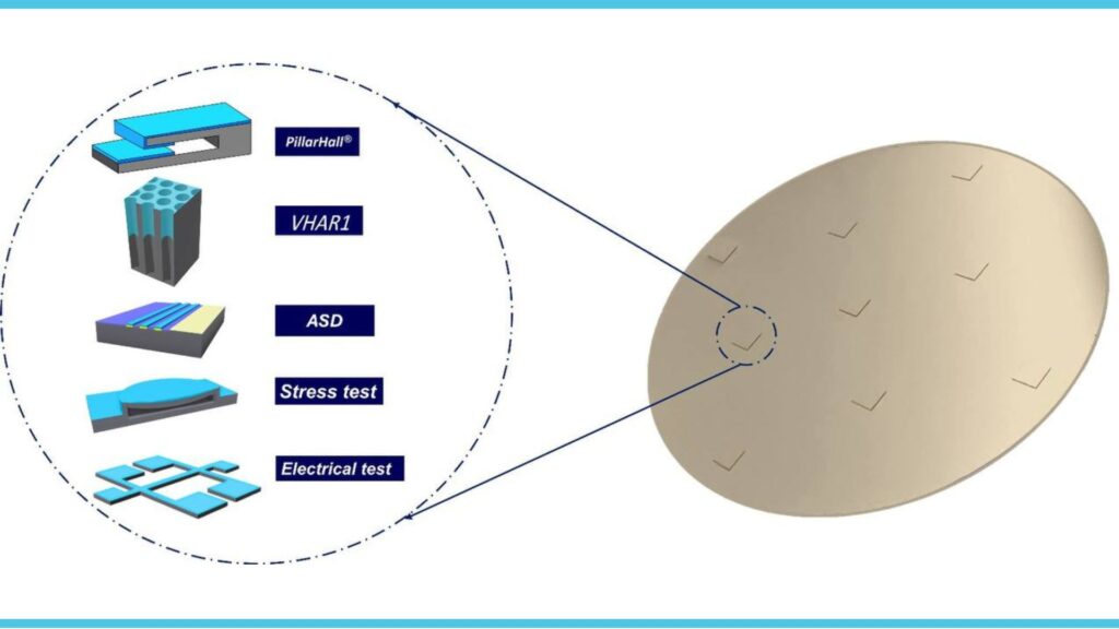
Chipmetrics 300 mm pocket wafer approach enables innovative test structures for fast and accurate qualification of critical thin film properties.
Semiconductor manufacturing presents a complicated challenge, demanding flawless execution across hundreds of process steps to achieve optimal product yields. With the intricate timeline stretching up to three months until a wafer reaches completion, the risk of undetected process excursions can potentially impact yield, performance, or reliability.
Hence, robust process monitoring emerges as an important facet within semiconductor manufacturing landscapes. While certain parameters can be directly understood from product wafers—such as defectivity, critical dimensions (CD), film thicknesses, planarity, and electrical tests—significant attention is also directed towards precise monitoring of tool performance. Careful qualification protocols are instituted to ensure adherence to specifications for each tool, confirmation tests conducted at predefined intervals or based on the volume of processed wafers.
Moreover, the demand for tool requalifications following tool-down events needs meticulous execution. Here, specialized test wafers assume a pivotal role. In certain instances, the utilization of test wafers proves more economically prudent than employing precious product wafers. Alternatively, test wafers may integrate specific test structures designed for enhanced process analyses, facilitating simpler SEM preparation and enabling early detection of even the slightest process deviations. For instance, PillarHall chips feature test structures facilitating the monitoring of ALD film penetration depths with aspect ratios reaching up to 10,000, without the need for x-sectional analysis and resulting in substantial time savings vis-à-vis conventional methodologies.
These structures, manufactured utilizing MEMS technologies typically incompatible with CMOS fabs and presently absent on 300mm wafers, necessitate a bridge. Addressing this void, Chipmetrics recently introduced a pocket wafer approach, embedding and permanently bonding test chips. This innovative strategy facilitates the expansion of the PillarHall approach to 300mm applications. Furthermore, it enables the combination of diverse test chip variants on a single wafer, streamlining a broad spectrum of process analyses—ranging from X-sections to film stress and electrical tests—previously requiring multiple wafer runs. This represents a transformative step in evolution of test wafers, and brings novel tool qualification and monitoring methodologies to enhance productivity and quality benchmarks within semiconductor manufacturing.